Research
Please visit the above links to have a more detailed look at our research projects. Below is a list of Centers that we are leading or affiliated with.
NSF MBM at UIUC - Miniature Brain Machinery
NSF STC EBICS at MIT/GT/UIUC - Emergent Behavior of Integrated Cellular Systems
NSF IGERT at UIUC - Cellular and Molecular Mechanics and Bionanotechnology
(download brochure)NIH Training Grant at UIUC - Midwestern Cancer Nanotechnology Training Center
(download brochure)NSF CiiT (I/UCRC) at UIUC - Center for Innovative Instrumentation Technology
NSF NSEC at OSU - Center for Affordable Nanoengineering for Polymeric Micro and Nanodevices
Research:
Growth and Characterization of SiGe Sub-Micron Self-Assembled Device Islands
Rashid Bashir, Abul. E. Kabir*, Kuo-Jen Chao#
*A. E. Kabir is with Process technology development group at National Semiconductor, Santa Clara, CA. where the growth of the films were done.
#Kuo-Jen Chao and C. Weitzsacker are with Charles Evans and Associates at Sunnvale, CA.
(Additional funding currently being pursued)
In this study, we report on the formation of self-assembled Si1-xGex islands by the selective chemical vapor deposition of highly strained Si1-xGex thin films (with x ~ 0.5) on patterned silicon wafers and the subsequent annealing of these thin films. Unlike previous studies, islands are formed during the thermal annealing of these thin films after the growth of the smooth continuos selectively grown thin films and not by direct growth of the islands. 50 - 150Å Si0.6Ge0.4 films are selectively grown on silicon wafers with an oxide pattern using chemical vapor deposition from germane, silane and HCl at 650°C and 40 Torr. In-situ annealing of the films at 750°C at 20 Torr for 6 minutes resulted in the formation of the islands. The composition of the films before annealing and islands formed annealing was investigated using scanning auger microprobe. The germanium fraction was found to decrease to about 20% in the self-assembled islands.
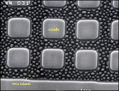 |
Figure: Angled scanning electron microscope picture of region B of wafer 2 after the thermal annealing subsequent to the growth. Anneal was performed at 750°C for 6 min at 40 Torr in hydrogen. Islands are formed in the regions between the oxide where the film was initially grown selectively. |
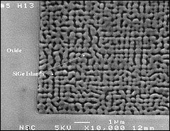 |
Figure: Angled scanning electron microscope picture in region A of wafer 3 after the thermal annealing (subsequent to the growth). Anneal was performed at 650°C for 25 min at 20 Torr in hydrogen. The islands clearly show order and regularity. |
References:
[1] R. Bashir, A. E. Kabir, Kuo-Jen Chao, and C. Weitzsacker, “Formation of Nanoscale Self-Assembled Si1-xGex Islands Using Chemical Vapor Deposition and Subsequent Thermal Annealing of Thin Metastable Films”, 41st Electronic Materials Conference, Santa Barbara, CA, June 30th-July 2nd, 1999. [abstract (pdf)]
[2] R. Bashir, A. E. Kabir, and K. Chao, “Formation of Self-Assembled Si1-xGex Islands Using Reduced Pressure Chemical Vapor Deposition and Subsequent Thermal Annealing of Thin Germanium Rich Films”, Applied Surface Science, 152, pp. 99-106, 1999. [manuscript (pdf)]
[3] K-J. Chao , A. E. Kabir , and R. Bashir, “Atomic Force Microscopy Study of Self-Assembled Si1-xGex Islands”, AVS 1st International Conference on Microelectronics and Interfaces, Santa Clara, CA., , Feb. 11th, 2000.
[4]R. Bashir, K-J Chao, and A. E. Kabir, “Atomic Force Microscopy Study of Self-Assembled Si1-xGex Islands Produced by Controlled Relaxation of Strained Films”, Journal of Vacuum Science and Technology-B, Vol. 19, No. 2, March/April 2001, pp. 517-522.