Research
Please visit the above links to have a more detailed look at our research projects. Below is a list of Centers that we are leading or affiliated with.
NSF MBM at UIUC - Miniature Brain Machinery
NSF STC EBICS at MIT/GT/UIUC - Emergent Behavior of Integrated Cellular Systems
NSF IGERT at UIUC - Cellular and Molecular Mechanics and Bionanotechnology
(download brochure)NIH Training Grant at UIUC - Midwestern Cancer Nanotechnology Training Center
(download brochure)NSF CiiT (I/UCRC) at UIUC - Center for Innovative Instrumentation Technology
NSF NSEC at OSU - Center for Affordable Nanoengineering for Polymeric Micro and Nanodevices
Research: >> Past >> NanoSensors for....
NanoSensors for DNA Detection:
1. Nano-fabricated Pores for DNA Conductance and Sequencing
H. Chang, R. Bashir
School of Electrical and Computer Engineering, Purdue University
F. Kosari, G. Vasmatzis
Mayo Clinic, Rochester, MN.
The general objectives of the work include initiating research in the newly emerging applications of MEMS to biology, combining the knowledge base from the silicon device processing and biological life sciences, and developing systems which can be used for the characterization and handling of individual poly-nucleotide molecules of DNA and mRNA. The ability of control and manipulate individual strands of DNA can have very powerful long-term effects in the area of nano-biotechnology. The use of DNA as molecular wires in a complex bio-electronic system, measurements of important properties of DNA, and realization of DNA/electronic interface devices are all important long term goals of the research described in this proposal. Silicon processing has been used to develop various Micro-electro-mechanical structures for bio-medical applications in the recent years. Specifically, in this work we propose to demonstrate the feasibility of a silicon-based micro-electro-mechanical-system which can be used for the characterization and sequencing of individual polynucleotide molecules including DNA and mRNA. Extremely small “nano-pores” (diameter < 50Å) will be formed in a very thin silicon membrane (thickness < 500Å) which separates two chambers. The thin silicon membrane will be formed either using selective epitaxial overgrowth of silicon and chemical mechanical polishing or LPCVD of silicon nitride. The pores will be formed to their initial size using e-beam lithography and dry gas phase etching. The final dimension of the pores will be achieved using controlled oxidation or deposition steps. An electric field will be applied across the membrane and the charged molecule under analysis will traverse through the pore from one chamber to the other. The chamber would be filled with a conducting solution. As the molecule traverses through the pore, the conductance measured across the membrane will change due to size constraints of the molecule with respect to the pore.
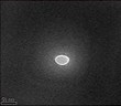 23 nm (1,000,000 X) |
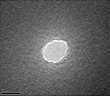 19 nm (1,000,000 X) |
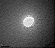 11 nm (1,000,000 X) |
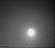 7 nm (1,000,000 X) |
 41 x 26 nm (300,000 X) |
 4 nm (1,000,000 X) |
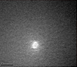
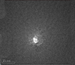
TEM pictures of pores fabricated in our lab |
||
The work was funded by Rockefellar Brothers Fund Biomedical Pilot Fund.
Now it is funded by NIH.
References:
[1] J. J. Kasianowicz, E. Brandin, D. Branton, and D. W. Deamer, “Characterization of Individual Polynucleotide Molecules using a Membrane Channel”, Proc. National Academy of Science, Vol. 93, pp. 13770-13773, November 1996.
[2] H. Chang, A. Ikram, M. Young, F. Kosari, G. Vasmatzis, A. Bhunia, R. Bashir, "A Microfabricated Device For Characterization Of Biological Species”, Proceedings of the MRS Spring Meeting, San Fransisco, CA. April, 2001.
[3] H. Chang, A. Ikram, T. Geng, F. Kosari, G. Vasmatzis, A. Bhunia, and R. Bashir, “Electrical characterization of microorganisms using microfabricated devices”, Journal of Vacuum Science & Technology B. v 20 n 5 September/October 2002. p 2058-2064
Funded by NIH and NASA INAC at Purdue
2. Nanowire Sensors for DNA Detection
Oguz Elibol, Dallas Morisette, Don Bergstrom, Rashid Bashir
The goal of this project is to demonstrate the capabilities of integrated nanowire biomolecular sensors, based on a fabrication approach that is compatible with modern VLSI semiconductor manufacturing. Our devices are fabricated using standard optical photolithography and silicon processing, combined with a novel silicon epitaxy technique that produces extremely thin layers of single crystal silicon-on-insulator (SOI). The process we use can produce both nanoscale channels and wires, suspended above an integrated gate. The resulting devices are illustrated schematically in Figure 1. Colorized SEM’s of the actual fabricated nano-wire devices are shown in Figure 2. By selectively doping the channel (or wires) the device can be made to operate as a resistor or a transistor, depending on the doping type. In either case, sensing is achieved by a change in conductance when an analyte adsorbs or chemisorbs to the surface of the wires. The final chips will include microfluidic systems that will direct the flow of liquid analytes to these sensors.

Schematic of Nanoplate/Nanowire Device Structure with Integrated Gate
[1] O. H. Elibol, D. Morisette, D. Akin, J. P. Denton R. Bashir, “Integrated Nano-Scale Silicon Sensors Using Top-Down Fabrication”, Applied Physics Letters. Volume 83, Issue 22, pp. 4613-4615, December 1, 2003